Heterogeneous intefration based on room temperature bonding technique
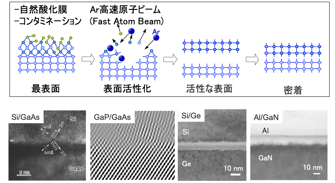
Surface activated bonding
Bonding is a core technique for fabrication and packaging of electronics. In particular, the room temperautre bonding has advantages including
・ Less damege to devices
・ integration of various materials including polymer with different coefficient of thermal expansoin
・ environmental-friendly process without long time annealing
・ suppression of misalignment owing to cooling step
・ avoidance of IMC formation
・ high heat resistance without liquid phase bonding interface
We researach and develope the device packaging technology based on surface activated bonding at room temperature.
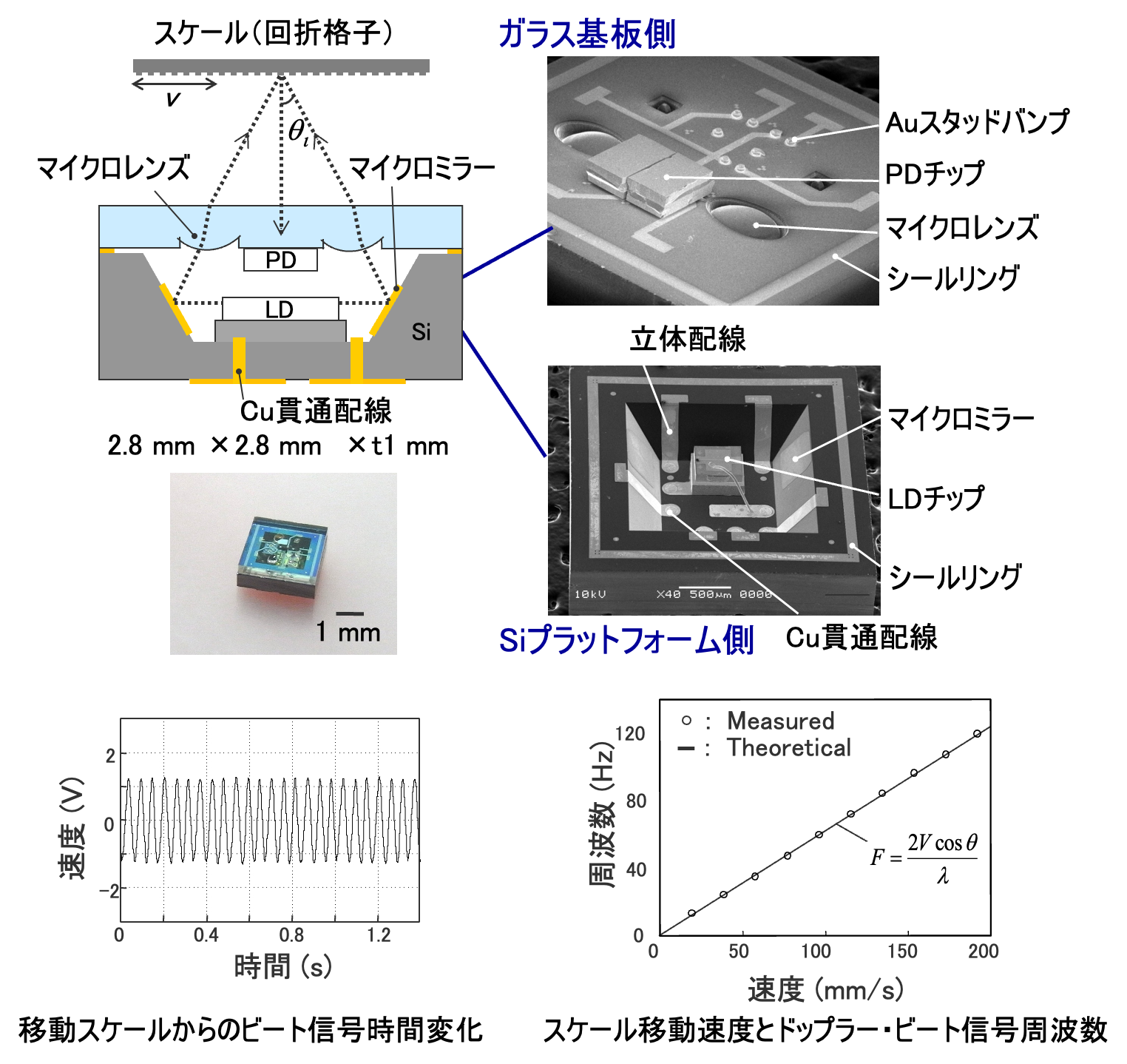
Small, light, and high functional integrated devices
3D integrated micro optical encoder
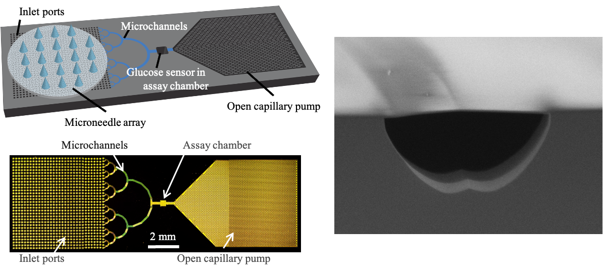
Sealing of microcfluidic device by room temperature bonding
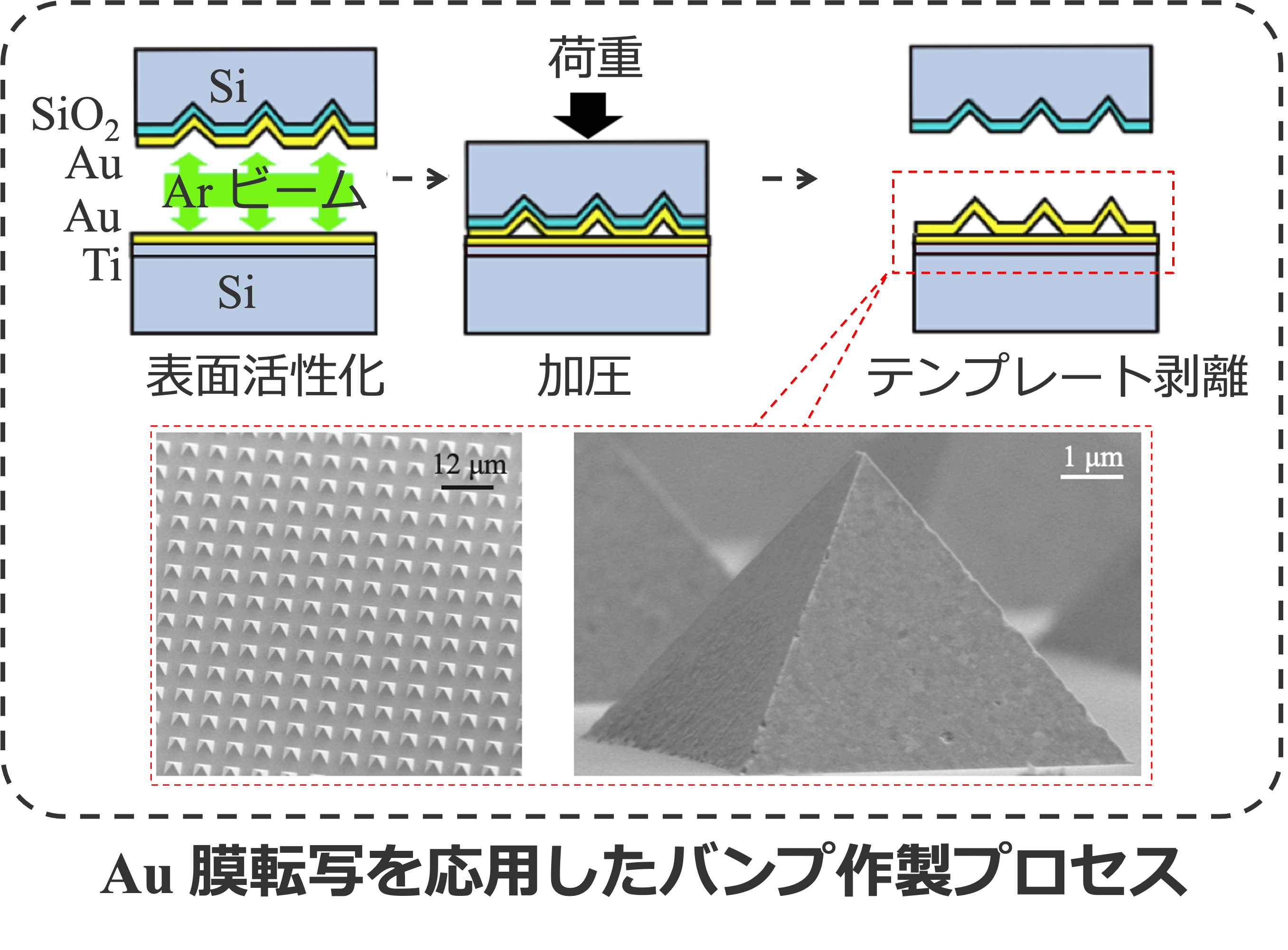
Smooting technique of the bonding surface for room temperature bonding
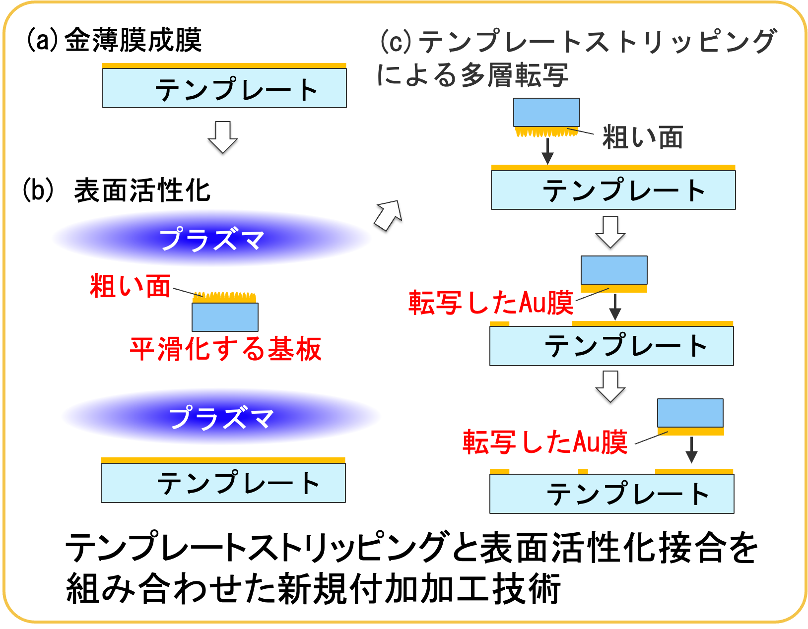
Smoothing by template stripping
Smooth surface is necessary for low temperature bonding. We develope a novel approach for smoothing technology of chip size, patterned, or Au materials which is difficult to smooth by CMP. We combine the template stripping techniquie, by which a thin metal film is transfered to target surface, and surface activated bonding technique for room temeprature bonding.
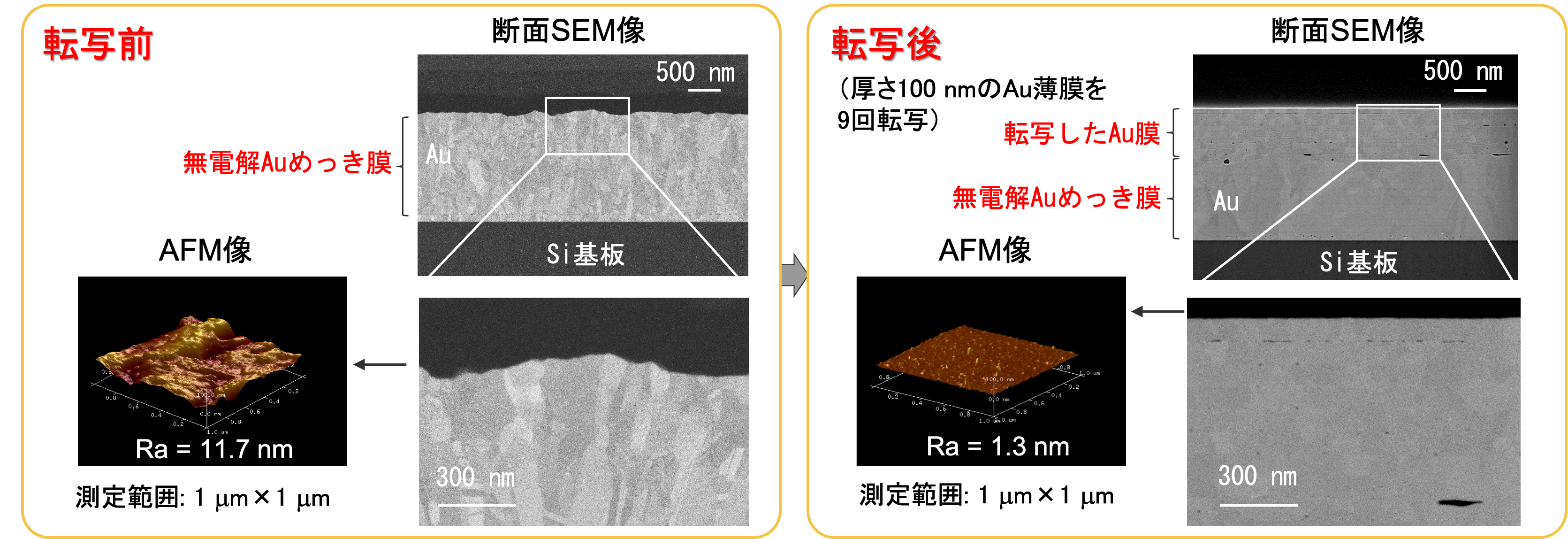
Smoothing of plated Au surface
Room temeprature wafer bonding via polysilazane
We have developed a new approach for room temperature wafer bonding through conversion of polysilazane into SiO2 bonding interface.
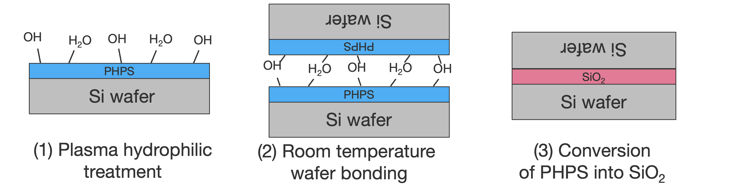
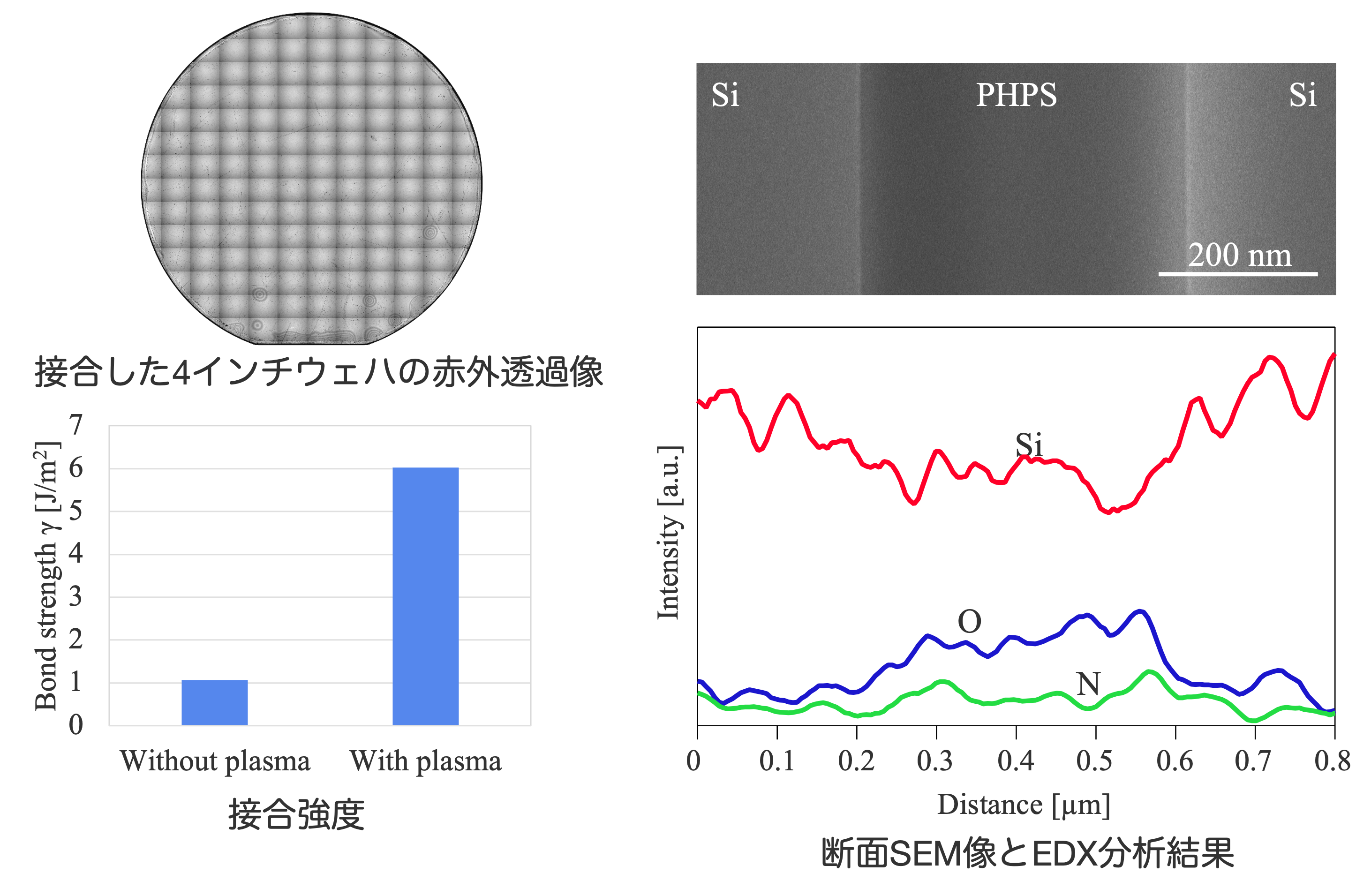
High bonding strength and good adhesion were achieved by the conversion reaction of polysilazane without thermal treatment.
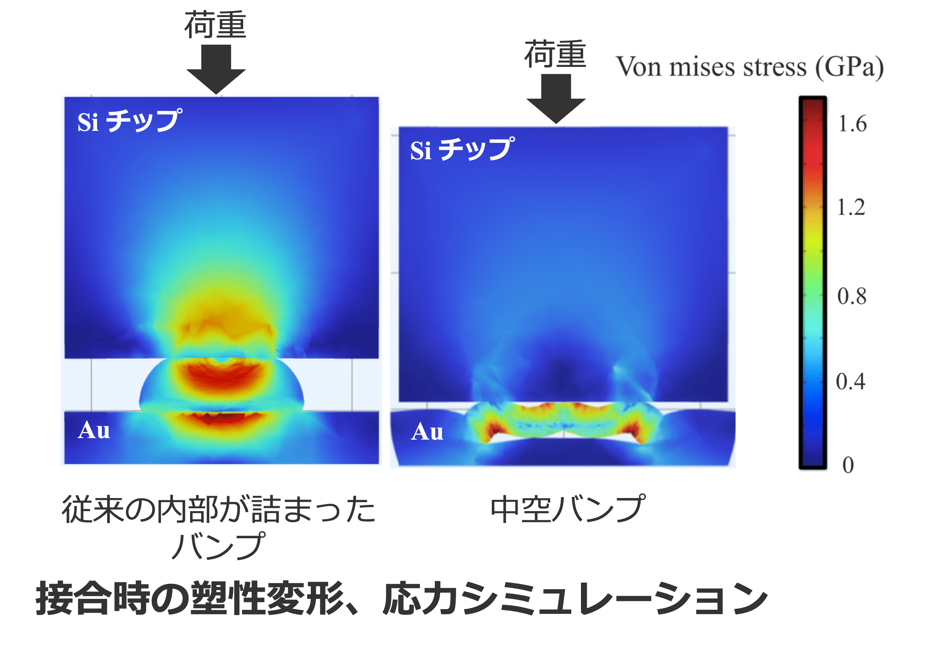
Low temperature bonding with small stress using Au hollow micro bumps
A new microbump has been developed for low temperature and low load bonding by facilitating plastic deformation of the bumps.